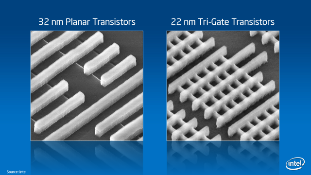
Intel announced a very important piece of semiconductor news in many years: the tri-gate transistor. The redesign of the 2D planar to the 3D tri-gate transistor is a fundamental change and will bring about big savings in efficiency and power consumption.
The tri-gate transistor is being produced starting at the 22nm manufacturing node and will be introduced with the upcoming Ivy Bridge CPUs. Intel will eventually include this technology in it’s entire processor portfolio from mobile to server.
The problem with the current planar transistors is that as they get smaller less current can squeeze through it. As the transistors get smaller the leakage current flowing through when the switch when it is off becomes indistinguishable from the current that is allowed to pass through it when the switch is on.
With the 3D tri-gate transistor above there’s a lot of gate surface area in contact with the semiconductor material. Because of this design structure more current can be transferred which the switch is on, and less current is permitted to leak when the switch is set to off. Besides being more power efficient this design creates a clear boundary between the on and off states. This allows the transistor to switch between states faster and gives room for higher clock speeds in future CPUs.
Intel claims that the 22nm tri-gate transistors can switch states between 18 and 37 percent faster than the 32nm planar ones (higher clock speeds). Alternatively the new design can reduce power consumption at current clock speeds by up to 50 percent.
Intel’s upcoming 22nm Ivy Bridge processor will use this new technology which is planned to go into mass production the second half of this year. This development will undoubtedly put Intel closer to ARM in terms of power consumption. Whether it is enough to push x86 processors into smartphones is another question which ramains to be answered.


